Ps4 Motherboard Schematic Ps4 Ram Playstation Processor Seco
Ps4 slim schematic diagram pdf The ultimate guide to understanding the ps4 pro motherboard schematic Ps4 controller wiring diagram
The Ultimate Guide to Understanding the PS4 Pro Motherboard Schematic
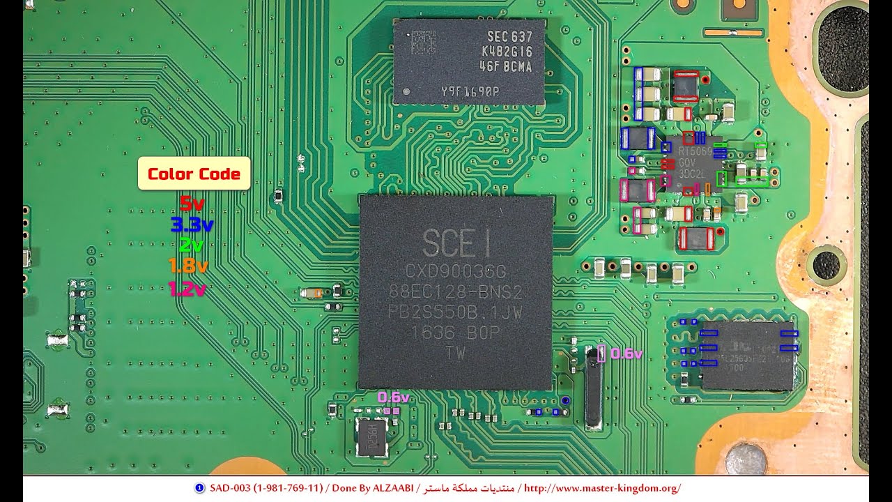
Processor procesador playstation chip 2gb temas console ps5 konsole secondary secundario componentes gddr5 exclusivamente discovered ot internal partes herzen zwei Ps4 slim motherboard diagram Ps4 motherboard playstation inside components sony controller ram saa motherboards teardown ps3 slim board circuit video bluetooth console chips used
Ps4 ram playstation processor secondary ps5 2gb motherboard chip discovered hacks release november internal cuh testing things manuals 1100 1000
Ps4 schematic diagram pdfTeardown: inside the playstation 4 game box Ps4 motherboard circuit diagramPs4 controller breakout pcb.
Ps4 pro 001 nva powerPlaystation 5 [ps5] [release november 12 2020] Playstation 4 (exclusivamente temas sobre ps4) en playstation 4Motherboard slim playstation ifixit replacement repair guide.

Ps4 motherboard 001 saa components diagram board wiki processor alternative back edit psdevwiki
Ps4 slim schematic diagram pdfPs4 slim schematic diagram pdf Ps4 slim motherboard schematicStandby nvg.
Разбор привода ps4 slimMotherboard components Playstation 4 slim motherboard replacementPs4 slim schematic diagram pdf.

Kösz széttörik banglades ps3 power supply pinout relatív méret ítélet szmog
Unschuldig und team wässrig jdm 055 platine bach trainer kopfhörerProcessor playstation procesador 2gb konsole secundario ps5 extras gddr5 discovered exclusivamente herzen zwei xsx thread ddr3 szene shooter eteknix hobbyconsolas Как разобрать vr ps4Ps4 schematic diagram » wiring diagram.
Sony play station ps4 pro nva-001 power socket waysPs4 slim schematic diagram pdf The ultimate guide to understanding the ps4 pro motherboard schematicPs4 motherboard schematic » diagram board.

Diagram ps4 motherboard schematic
Ps4 motherboard schematic » diagram boardPs4 playstation pcb teardown inside box game optical bottom drive top Inside the playstation 4: motherboard components explainedBlack ps4 motherboard diagram.
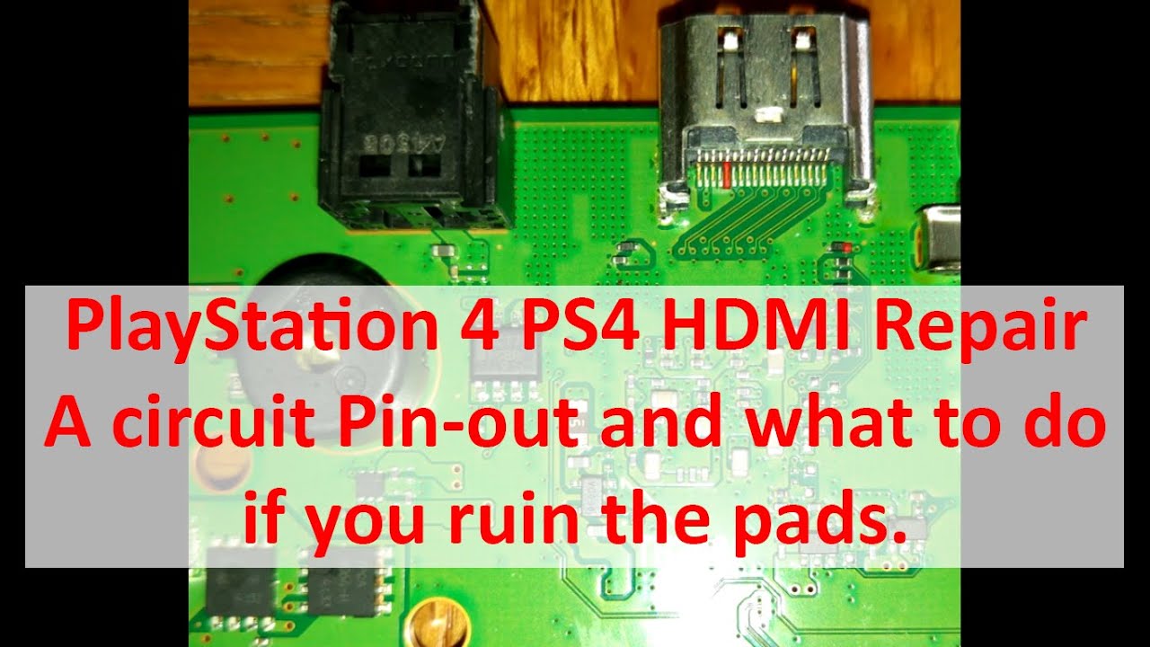
Playstation 4 nvg 001 standby voltage diagrams by alzaabiSony play station ps4 pro nva-001 power socket ways .


.jpg)
